White-Box AI Agent for Semiconductor Fab Engineering Diagnosis & Validation

Intelligent Equipment. Pinpoint Field Diagnosis. Faster Sign-Off & Lot Cycles.

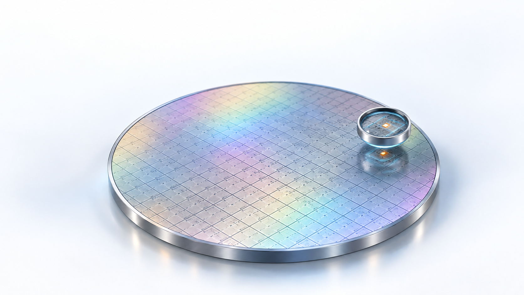
Engineering diagnostic concept scene with full wafer and local magnified review region

OUR MISSIONExploring AI-era semiconductor engineering analysis and verification.

See How Agent Investigates
01 / DIAGNOSTIC SCENARIOS

Solving Four High-Frequency Fab Challenges

01 · NEW TOOL CALIBRATION

Fewer Monitor Wafers,
Calibrate & Sign Off in Days

From a single monitor wafer, directly compute exact focus and dose adjustments—ending weeks of blind trial-and-error wafer runs.

-70% Tool qualification cycle · Target reached in 1-2 runs
02 · CROSS-STEP DEFECT ATTRIBUTION

Compare Pre & Post Images,
Pinpoint Step Responsibility on the Spot

Overlay pre-step and post-step inspection maps of the same wafer to automatically subtract inherited defects and isolate net-new additions.

100% Isolated Upstream defects filtered · End cross-team blame games
03 · FALSE-ALARM RETUNING

Spiking Tool False Alarms,
Retuned Locally in One Click

Process changes often cause inline inspection models to flag good wafers. Without exporting sensitive wafer images, field engineers recalibrate thresholds on-site in one click.

18.4% -> 1.2% False-alarm rate restored on-site · Zero data egress
04 · DOCUMENT EXPERIENCE REUSE

Learn from Past & New Documents,
Never Repeat Solved Mistakes

Most issues during tool installation or Fab production have happened before. The platform extracts and learns experience from existing and newly accumulated documents to guide engineers on the spot.

Continuous Learning Extracts from existing & new docs · Instant solution reuse

How does it advance investigations?

02 / AGENT IN ACTION

Let Agent operate the workspace.
Keep every step visible to engineers.

The Agent inspects imagery and prior runs, executes standard checks first, and runs targeted analyses on demand.Grounding decisions in accumulated evidence and verified engineering method specs.

01 / Ingestion (300mm) 4s
02 / Zoom-In Cluster 5s
03 / FDC Telemetry 5s
04 / SEM & 8D Review 5s
Continuous autonomous loop · Zero-click
Autonomous Pipeline Active KLARF_STREAM: Lot-2026-N5-042 · STEP: AEI_MET1 · TOOL: TEL-Etch-04
✓ 1. Zero-Friction Klarf/Log Ingestion
➔
✓ 2. Same-Wafer ADI↔AEI Registration
➔
⚡ 3. In-Situ FDC Causal Telemetry
➔
○ 4. 8D Sign-off & Recipe Compensation
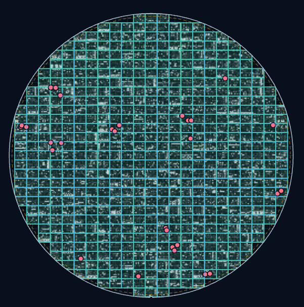
KLARF: 300mm Full Map
300mm Silicon Wafer Inspection Map
● Defect Cluster
Die (18, 4) · R: 147.2mm
118 Added Defects (83.1%)
MAG: 1.0X FOV: 300mm · 142 Total Defects
Grid: SEMI M1 Die-Pitch (0.1µm): X: +146.8mm, Y: +22.4mm Edge Zone (R=147.2mm) Added Polymer (8 pts)
All Defects (142)
Post-Etch New (118)
ADI Baseline (24)
Radial Defect Density D(R) & Cumulative Pareto Curve
R > 145mm Spike (83.1%)
0.0 2.0 4.0 6.0 0% 80% 0-30 30-60 60-90 90-120 120-135 135-145 145-148mm 5.42/cm² 148-150 2mm Exclusion
Total Defects: N = 142 Edge Ratio: 83.1% Skewness: +4.82 Attribution Confidence: p < 0.001 (Etch Signature)
ETCH-04 Chamber 3 In-Situ Sensor Telemetry (ESC He-Leak & Temp)
t = 42.4s Helium Leak Trigger
BT (0-15s) ME1 (15-42s) ME2 (42-75s) [FAULT] OE (75-90s) 42.4s Pressure Drop -33% 0s 42s 75s 90s
● ESC Backpressure: 12.0 → 7.8 Torr (LCL Breach) ● Focus Ring Temp: 64.5 → 68.3°C (+3.8°C) Diagnosis: Chamber 3 ESC Seal Ring Wear
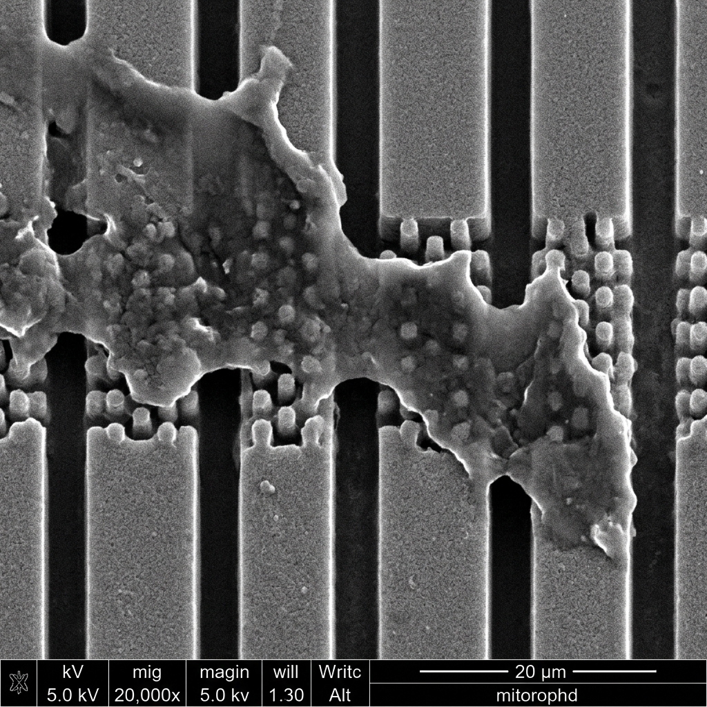
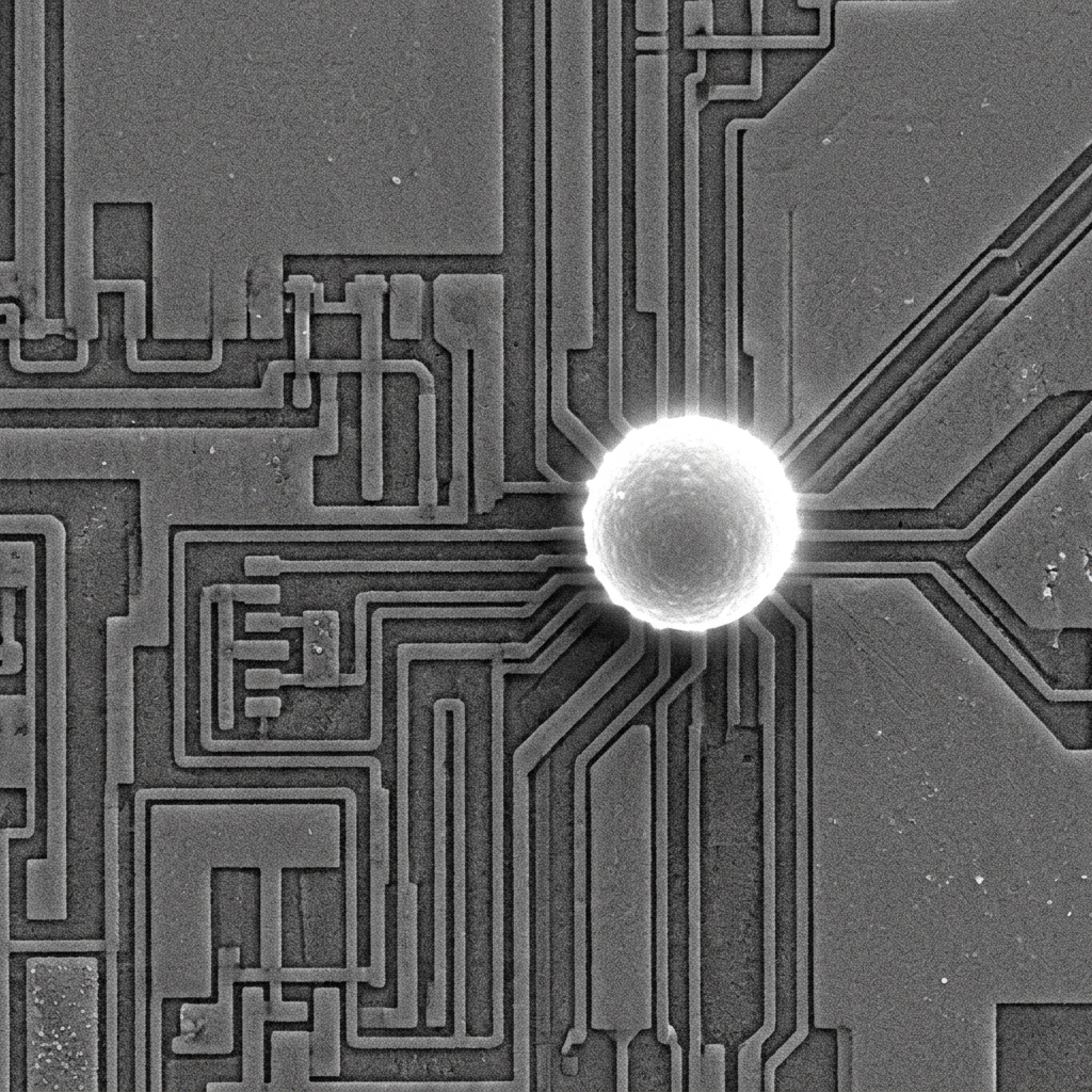
Post-Etch Polymer Residue SEM
20 µm
5.0 kV · 20.0 kX · SEI
Edge Etch Polymer Residue 98.6%
Klarf: #24 Polymer Die: (18, 4) · R: 147.2mm
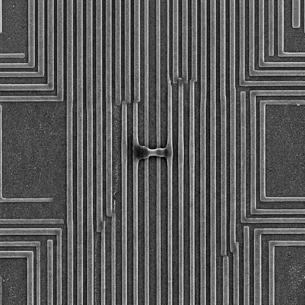
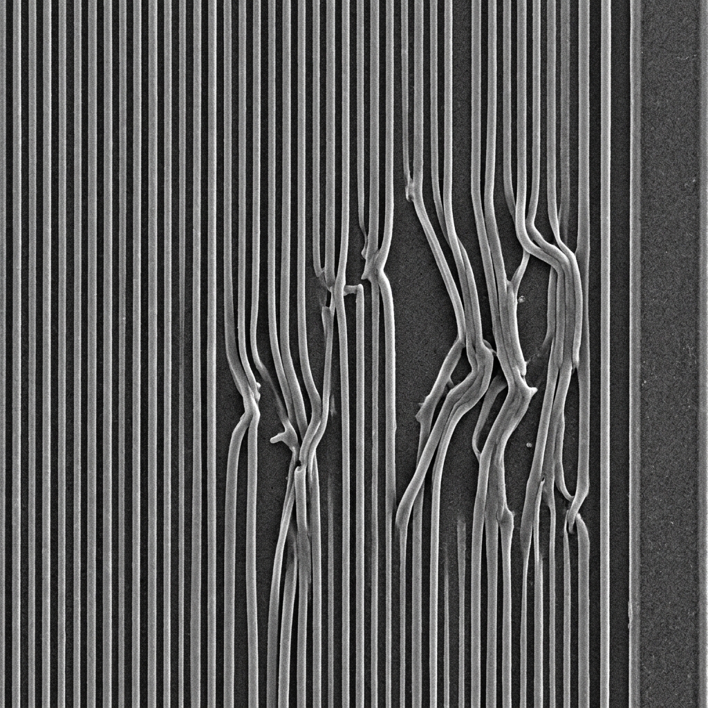
Line Bridge Short SEM
100 nm
1.0 kV · 80.0 kX · InLens
Nanoscale Line Bridge 96.4%
Klarf: #22 NanoBridge Die: (17, 3) · R: 146.1mm
Chamber Particle Defect SEM
2 µm
2.0 kV · 50.0 kX · BSE
Chamber Ceramic Particle 99.1%
Klarf: #10 Fall-on Die: (11, -2) · R: 92.5mm
EUV Pattern Collapse SEM
200 nm
1.0 kV · 75.0 kX · SEI
Pattern Collapse 94.7%
Klarf: #35 Structural Die: (16, 5) · R: 145.8mm
Lot: W402-A-042 Wafer: #18 Total Defects: 142 (New: 118)
Grid: SEMI M1 Die-Pitch (0.1µm)
WP
WaferPilot Copilot Online
Fab Collaborative AI Copilot · On-Prem Causal Brain
Zero-Egress Private Deploy
Defects spiked along the edge of this wafer. Is it litho defocus or an etch issue?

Analysis complete (micron-level ADI ↔ AEI registration):

  • Prior ADI litho baseline: 24 defects (normal baseline, Overlay < 0.8nm)
  • Post-etch AEI detected: 142 defects
  • Differential new: 118 defects (83.1%), tightly clustered in edge 5mm ring

Definitive attribution: Post-etch process excursion; litho defocus and dose shift ruled out.

🔍 Dynamic Zoom-In to Edge Defect Cluster
Can we pinpoint the exact tool, chamber, and sensor parameter drift?

Causal correlation & in-situ FDC sensor drill-down:

  • Responsible tool: ETCH-04 / Chamber 3
  • Root-cause timing: At 42.4s (Main Etch 2 step), ESC helium backpressure suffered a 33% step leak (12.0 → 7.8 Torr);
  • Loss of conductive cooling caused edge temperature to jump +3.8°C, driving excessive polymer deposition.
📊 Open Chamber 3 Histograms & FDC Telemetry
Provide inspection actions and recipe offsets for this excursion.

Matched against historical 8D causal graph, dispatching instant SOP:

  • 1. Immediate inspection: Check Chamber 3 ESC inner seal O-ring wear and leakage;
  • 2. Emergency recipe offset: Adjust edge zone power compensation ΔP_Edge = -1.8%;
  • 3. Correlated screening: Inspect remaining 4 wafers in lot for edge focus ring drift.
🔬 Inspect High-Res SEM Defect Micrographs
01 / VISIBLE ACTIONS

Visible Actions

Regions of interest, tool calls, and computed metrics displayed side-by-side on one screen.

02 / EVIDENCE-DRIVEN

Evidence-Driven

Every hypothesis update and next step is justified by accumulated observations and specs.

03 / ENGINEER IN CONTROL

Engineer in Control

Review, adjust parameters, or take over control at any point; open questions remain highlighted.

How does it integrate into my existing environment?

03 / PRIVATE DEPLOYMENT & INTEGRATION

Runs inside your perimeter,
integrates into existing workflows.

Deployment Options: Fab Private Cloud / On-Premises · Equipment Edge Computing.

PRIVATE DEPLOYMENTPrivate Architecture Schematic
  • FABFab Private Cloud or On-Premises
  • EQUIPMENT SUPPLIEREquipment Edge Computing
Conceptual scene of wafer Fab cleanroom and engineering computing environment
PRIVATE / Customer EnvironmentYour Computing Environment

Data and computation stay entirely within customer perimeter.

Private Execution
Data Stays on the Customer Side
Local InferenceLocal ComputeLocal Records
Existing Tools & EquipmentTypical Unit Steps · Collaborative Analysis
Lithography
Deposition
Etching
Metrology & Inspection
Existing Fab DataWafer Images · Defect RecordsRecipe · Config · Components · Log
WaferPilotCustomer Environment · White-Box Agent
Agent InvestigationObjectives · Next Actions
Method SpecsApplicable Specs · Method Grounding
Scientific ComputingPipelines · Algorithms & Metrics
Memory & EvidenceInvestigation Context · Run Traces
Engineering method specs and traces remain securely in customer perimeter
Engineering TeamsEE / PE / PIE · Field Support
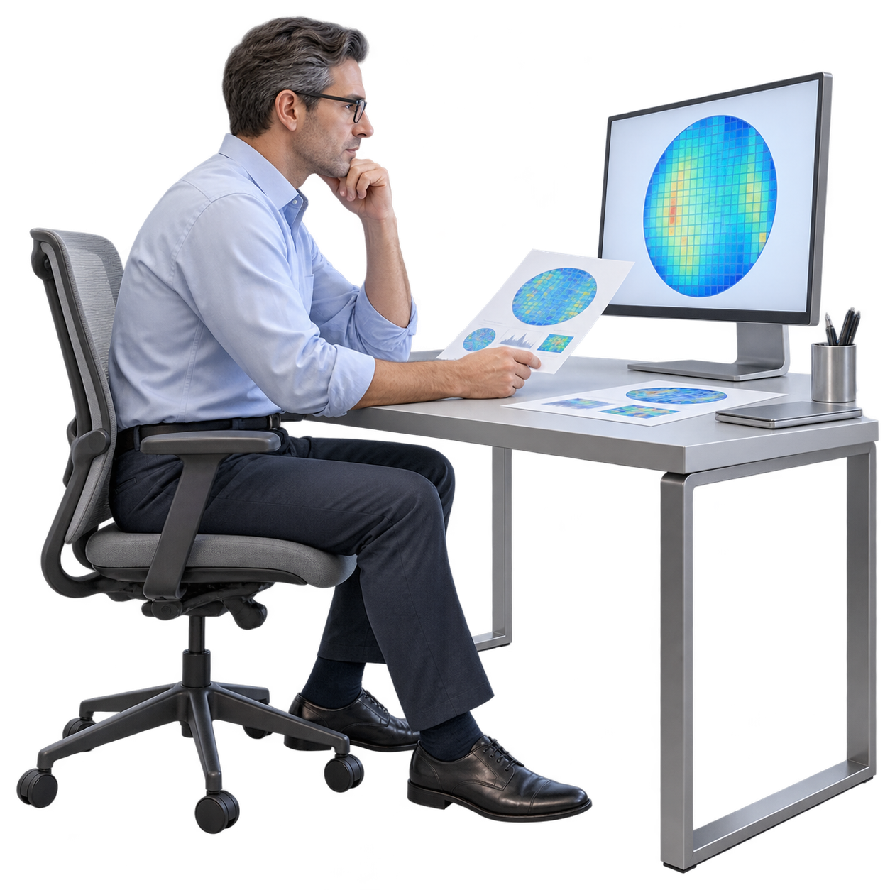
Conceptual illustration of semiconductor engineer reviewing wafer metrics at fab workstation
Back to Engineering WorkflowAuditable Findings.
Verifiable Recommendations.
Engineer Review · Schedule Validatione.g., Cross-check inspection recipes and upstream steps
Engineer review and validation results inform subsequent investigation rounds
Update Hypotheses

Equipment, data, and engineers collaborate continuously inside the same Fab.

Data & Workflow IntegrationHow does it connect to existing tools and datasets?View Synergy Flow

Transforming massive wafer data into engineering insight.

Aligning lot, time, coordinate, and recipe versions first, then collaborating with existing tools to deepen PE and PIE investigations.

FAB DATA / Cross-Step Investigation
  1. 01 Massive Data
  2. 02 Synergy Analysis
  3. 03 Audit & Update
  4. 04 Engineering Insight
Existing WorkflowsTypical Unit Steps · Sampled per Sampling Plan
DepositionDEPOSITION
LithographyLITHOGRAPHY
EtchingETCH
CleanCLEAN
CMPPLANARIZE
MetrologyMETROLOGY
Deposition Inspection
Lithography Inspection
Etch Inspection
Clean Inspection
CMP Inspection
Metrology Readings
Inspection Tools·Image & Defect Data·Yield Management System·Custom Analytics / Python
Collaborative Analytics Layer

WaferPilot

Align · Compare · Correlate · Model on Demand

Observe→Correlate→Analyze on Demand→Review↺
06 / 06

Feeding verified discoveries into the next validation cycle.

Handing candidate correlations, raw evidence, and recommended validation steps directly to PE and PIE.

Finding 01 · Cross-Step Spatial Distribution Delta→Finding 02 · Candidate Tool Correlation Pending Validation
Candidate Correlations / Pending Engineering ValidationSynthetic Chart
Tool State (Normalized)Image Features
Retaining provenance, computation parameters, and open questions
PE
Unit Step & Tool InvestigationAudit Clues · Schedule DOE
Grounded DiscoveriesReturn to Engineering Workflow
PIE
Cross-Step & Integration InvestigationUnderstand Correlations · Advance Verification

How does it help engineers resolve issues?

04 / ENGINEER VALUE

Turn raw data,
into grounded engineering recommendations.

Automates routine analysis across more wafers, time windows, and operating conditions, surfacing valuable clues and candidate causes. Engineers inspect evidence layer-by-layer, steer investigation directions, and advance findings into tuning and validation plans.

Engineer Workbench / Recommendations & EvidenceWorkbench Schematic
Wafer ImagesFull Wafer · Local ROI · Multi-Wafer
Metrology DataDistributions · Trends · Time Windows
Tool RecordsRecipe · Chamber · Sensor Traces
Semiconductor engineer reviewing diagnostic recommendations and underlying evidence on unified workbench
Engineer Review · Schedule Tuning & DOE
Continuous Ingestion into WorkbenchAnalysis & Recommendations to Guide Decisions
  • Patterns & Deltas

    Across Wafers · Time Windows · Process Conditions

  • Candidate Causes

    Supporting & Opposing Evidence · Pending Checks

  • Troubleshooting & Tuning Advice

    Priority Checks · Parameter Directions · Validation Steps

Complete Investigation Traces

Observations → Checks → Computations → Findings → Recommendations

Engineers Retain Full ControlReview · Adjust · Take Over
  1. 01

    Automate Routine Analysis

    Executes defined inspection routines, eliminating repetitive data extraction, coordinate alignment, and manual formatting.

  2. 02

    Cover Greater Data Breadth

    Structures comparisons across wafers, historical time windows, and operating splits to expand investigative coverage.

  3. 03

    Surface Actionable Clues

    Aggregates spatial patterns, parameter deltas, and candidate causes to support the next check and engineering proposal.

  4. 04

    Full Traceability & Control

    Inputs, method specs, quantitative metrics, and decision rationale remain fully auditable, adjustable, and steerable.

Automate Routine Analysis

Executes defined checks and computations automatically to reduce repetitive manual overhead.

01 / 04

What do I receive at the end?

05 / DELIVERABLES

Diagnostic reports and recommendations,
backed by complete investigative evidence.

A comprehensive report outlining current diagnosis, recommended actions, and validation procedures, with every suggestion tied to analytical traces, evidence, and open questions.

  1. Tool Qualification
  2. Process Excursion
  3. Model Diagnosis
Report Deliverable Overview
Tool deviation report scene: test wafer and golden reference comparison
Tool Ramp QualificationEE / PE · Equipment & Process Engineering
Unified Engineering DeliverableOne Investigation,
Complete Package.
  1. 01Diagnostic Report
  2. 02Recommendations
  3. 03Validation Plan
  4. 04Full Evidence Traces
ENGINEERING REPORT01 / 03

Tool Qualification Assessment & Tuning Recommendations

Diagnostic Report
Chamber matching deltas, cross-lot stability, and process window compatibility; candidate factors and supporting evidence.
Recommendations
Priority inspection items, tuning sequence, and grounded parameter adjustment directions.
Validation Plan
Defined reference baselines, re-measurement conditions, and pass/fail criteria for matching, stability, and compatibility.
Full Evidence Traces
Primary and reference datasets, condition snapshots, check/computation logs, and non-excluded candidate factors.
Evidence chain connecting findings to raw data and execution tracesRaw DataMethod SpecChecks & ComputeAnalysis FindingsRecommendations

Where do its engineering judgments originate?

06 / ENGINEERING EXPERTISE

Codify engineering experience,
into actionable Agent method specs.

Derived from process specs, equipment manuals, standard analytical practices, and cleanroom field experience,
forming reviewable, version-controlled method specs validated against precise applicability boundaries.

EXPERTISE / From Experience to ActionMethod Codification Flow
  1. 01 Field Experience
  2. 02 Expert Review
  3. 03 Spec Execution
  4. 04 Continuous Asset
Senior semiconductor engineer reviewing wafer heatmaps and historical investigation cases at workstation
Verify scan area first,
compare defect distributions second.
Engineer Knowledge FoundationsProcess Specs · Tool Manuals · Field Practice
EXPERTISE PACKAGE

Wafer Comparison Spec

v1.1
01
PrerequisitesComparable Scan Area
02
Method ProtocolVerify First, Compare Second
03
Evidence StandardAuditable Provenance & Metrics
Expert Verified
Reviewable · Editable · Version-Controlled

Team Knowledge AssetSpec Files · Protocols & Boundaries

Agent Workspace
HARNESS / Execution Runtime
Method Spec+Current Data+Analysis Tools
Scan Area Verified
Audit Area→Compare Patterns→Store Traces
Active Basis · Method Spec v1.0

Agent ExecutionSpecs Guide Action · Traces Stored with Output

New cases undergo expert review to enter next spec release
04 / 04

Verified experience fuels the next investigation.

Retains current investigation evidence, audits novel failure modes and methods, and publishes updated spec packages.

Deep DiveMethod Specs, Runtime Harness & ExtensibilityExpand
From experience to execution, and on to next-round reuse.Method Architecture Overview
01 / EXPERIENCEFab ExperienceSpecs · Manuals · Expert Judgment
02 / REVIEWCodification & ReviewEngineer Verified Protocols
03 / SPECMethod Spec FilesVersioned Knowledge Packages
04 / HARNESSRuntime HarnessSpecs · Data · Compute Tools
05 / EXECUTETask ExecutionAnalysis & Evidence Linked
06 / REUSEAudited Asset ReuseAvailable for Future Investigations
01 / 06

Starting from verified engineering sources and real fab problems.

Ingests process specifications, equipment manuals, and standard analytical SOPs; historical lots refine and harden rules.

method-sources.mdSource Grounding · Retaining Original Evidence
CASE
Engineering Problem
Spatial deltas between test and golden reference wafers
Experience Sources
Process specs, equipment manuals, standard SOPs, and expert heuristics
Engineering Judgment
Verify comparability first, interpret spatial distributions second
Applicability Bounds
Raw defect count delta alone does not prove process causation
Experience preserves origin; methods preserve applicability conditions.
WaferPilot Agent HarnessEngineering Runtime Framework
EXPERTISE PACKAGEActive Spec ReleaseMethods · Conditions · Evidence Standards
AGENT + RUNTIMEEngineering Judgment & Step VerificationCurrent Target · Data · Available Tools
WAFER ANALYSISWafer Investigation & EvidenceSpatial Review · Scientific Computing · Image Re-inspection
Awaiting expert-reviewed specs and active task integration.
New Cases & Validation OutcomesCandidate Findings → Expert Review → Spec Release → Next-Round Reuse
SAME HARNESS / NEW SPECS & TOOLS

One architecture, scalable to new engineering domains.

Method specs govern how judgments are formed; tool contracts define what actions can be executed. New engineering tasks simply plug in validated tools.

Wafer Image Spatial AnalysisActive Production Pilot
Defect Model Recovery & TuningExpansion Track
Recipe Parameter StudyExpansion Track

Wafer Analysis: Comparability specs, scientific computing tools, and evidence standards together power continuous investigation.

Experience belongs to the engineering team.

Codifies senior engineers' intuition and historical lot post-mortems into transparent, reviewable, and reusable team assets.

Specs guide every step of the workflow.

The Harness bridges specifications with ingested lot data, compute tools, and runtime verification; the Agent operates strictly within valid bounds.

Capabilities scale cleanly through specs.

Expand to new engineering tasks with modular spec packages, tool contracts, and benchmark lots while sharing the proven runtime harness.

Engineering expertise is managed as modular specs, published after expert review, and reused across future investigations.

ArchitectureHow Experience, Computing, and Evidence CollaborateView Architecture
PURPOSE-BUILT AGENT ARCHITECTURE

Designed specifically for
semiconductor image analysis.

TranslatingFab engineering expertise and senior analytical methodsinto applicability prerequisites, scientific computing routines, and rigorous evidence standards. Our Agent architecture advances along these engineering constraints to form a closed-loop investigation.

FAB ENGINEERING EXPERTISE

Understanding the cleanroom: knowing what questions to ask.

Incorporates tool state, recipe parameters, review optics, and comparison goals into the run, pinpointing which clues warrant DOE and what data must be fetched.

SENIOR ANALYTICAL METHODS

Definitive methods: knowing how to validate hypotheses.

Verifies population sample sizes, active inspected areas, analysis metrics, and baseline definitions to clearly distinguish observations from engineering explanations.

Method specs & applicability conditions · Engineering expertise guiding every cycle
AUTONOMOUS AGENTInvestigation & PlanningInspects available data, selects next action, and steers trajectory based on quantitative metrics.
SCIENTIFIC EXECUTIONAnalysis & Scientific ComputeExecutes rigorous algorithms on defined inputs, returning fully auditable calculations.
EVIDENCE & PROVENANCEFindings & Evidence TracesLinks raw wafer imagery, computational formulas, result revisions, and remaining evidence gaps.
Observe→Select Action→Execute→Verify→Update
Engineer · Confirm scope, pause, intervene, review findings, and schedule DOE

How do I audit its conclusions?

07 / EVIDENCE & AUDITABILITY

White-box AI Agent:
every recommendation backed by verifiable evidence.

From full-wafer imagery and recipe parameters to actionable engineering recommendations.
Inputs, method specs, computations, and execution traces are auditable layer by layer.

WHITE-BOX AGENTDual-Source Input · Auditable Engineering Evidence
Recommendations & EvidenceDual InputsMethod SpecsScientific Compute
Data & Compute Relations Hypotheses Pending Validation
Engineering AdvisoryAudit Variations First,
Isolate Causes Second
Inspection & Unit Steps · PE / PIEScreen candidate hypotheses before scheduling validation DOE
FINDINGOuter Ring Defect ConcentrationImage Review · Finding F-02
VALIDATIONCandidate Hypotheses Pending ValidationEvidence Gap Logged · Next Check Scheduled
CALCULATIONScientific ComputingRadial Statistics · Formulas Verifiable
PIPELINEChecks & ExecutionStandard Checks · Run Traces
INVESTIGATIONObservation & AuditInspected Scope · Corresponding Imagery
Full WaferDie BlockLocal ROISOURCEWafer ImagesFull Wafer → Die Block → Local ROI · Provenance Traceable
RecipeComponentsConfigCONTEXTRecipe ContextVersion · Tool · Unit Step · Timestamp
METHODSelect Method SpecDomain Grounding · Prerequisites Verified
EXPERTISEFab Specs & SOPsExpert Verified · Spec v1.0
From inputs to recommendations,
every layer of evidence opens automatically.
02 / 04

Every investigative branch leads directly to its underlying evidence.

WHITE BOXEvidence Retained with Findings
Traceable InputsImage and recipe context snapshots
Grounded MethodsDomain expertise and verified applicability bounds
Verifiable ComputeStandardized formulas and statistical parameters
Logged ExecutionTool call parameters and result revisions
Engineering Advisory

Confirm temporal deltas before isolating root causes.

Audit inspection conditions and intra-wafer progression first, then leverage recipe and tool logs to isolate candidate hypotheses. Recommended parameter adjustments require direct empirical evidence and validation DOEs.

Advisory Bounds & ConfidenceSpatial Distribution Quantified · Root Cause Pending Validation

Retains supporting evidence, gaps, and non-excluded candidate hypotheses. Recommendations provided for engineer review; correlated leads still require validation.

What engineering experience do we want to deliver?

08 / OUR MISSION

Exploring the next generation of
semiconductor analysis and validation.

Starting from Fab image analysis and yield learning, we bring engineers and specialized AI agents onto a unified workbench to investigate continuously, compute rigorously, and verify every finding together.

Transforming one-off reports into an ongoing engineering journey. New problems, fresh lot data, and emerging discoveries connect seamlessly inside the same shared context.

Evaluate an authentic investigation on your historical lot.

Define the engineering problem, inputs, and target deliverables for your team to assess incremental ROI.

View Pilot Preparation Guide